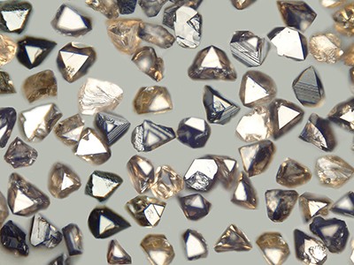
H-BN: Nature's “White Graphite”
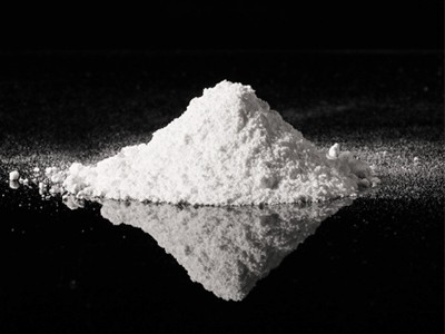
H-BN, a material with a hexagonal network of layers formed by sp² hybridization of boron and nitrogen atoms, has been nicknamed “white graphite” because of its white appearance and similar properties to graphite. As the only naturally occurring crystal of boron nitride in all its phases, h-BN is not only extremely hard and wear-resistant, but its layered structure also allows the layers to be bonded to each other by van der Waals forces, displaying unique physical and chemical properties.
Superior performance: the double advantage of hardness and insulation
The hardness of hexagonal boron nitride is second only to diamond, which makes it stand out in application scenarios requiring high strength and wear resistance. At the same time, as an insulator, h-BN has a band gap of up to 5.9 eV, which means it is ideal for the fabrication of tunneling barriers and UV-emitting light sources. In addition, h-BN has good thermal conductivity and chemical inertness, and is able to maintain stable performance in harsh environments such as high temperature, high pressure, and corrosion, which provides a solid foundation for its application in a variety of fields.
Bright star in the field of two-dimensional materials
In the field of two-dimensional materials, hexagonal boron nitride plays a pivotal role with its unique properties. Taking graphene as an example, when graphene is prepared as a field effect transistor on a silicon wafer, although it can show high carrier concentration and mobility, the effect is not optimal. This is because single-layer graphene is inherently soft and prone to wrinkles and bubbles, while the silicon wafer substrate has a large degree of undulation, and these defects can significantly affect the performance of graphene. In contrast, h-BN as a substrate can significantly reduce the disorder on the graphene surface and reduce the aggregation of electrons or holes, thus controlling the energy shift of the Dirac point and enhancing the electrical properties of graphene. Experimental data show that the carrier mobility and carrier uniformity of graphene prepared on h-BN have nearly an order of magnitude improvement compared with that of silicon wafer substrate.
BN(China) Technology: Innovation Leads to the Future
In the field of R&D and application of hexagonal boron nitride, BN(China) Technology is undoubtedly the industry leader. Relying on its profound accumulation in the whole industrial chain of boron nitride and carbon materials, BN(China) Technology has successfully launched a number of high-quality hexagonal boron nitride products. These products not only inherit the excellent performance of h-BN, but also further enhance its application effect and market competitiveness through BN(China) Technology's unique process and innovative technology.

At present, BN(China) Technology's h-BN products are synthesized by advanced continuous calcination equipment, with an annual production capacity of 1,000 tons, stable product performance, strong batch supply capability and outstanding cost advantage. Four specifications are available for you to choose from: PBN700 (purity ≥99.5%), PBN500 (purity >99%), PBN300 (purity >98%), PBN100 (purity >97%), and the four products are available with a crystalline particle size of 1-5 μm, and a powder particle size of D50 between 4 μm and 20 μm. These four specifications have been successfully applied to boron nitride ceramics, high-temperature coatings, mold release agents, lubricants, thermally conductive fillers, high-temperature insulating materials and other industries.
